HY2143-DA1C
Diagram
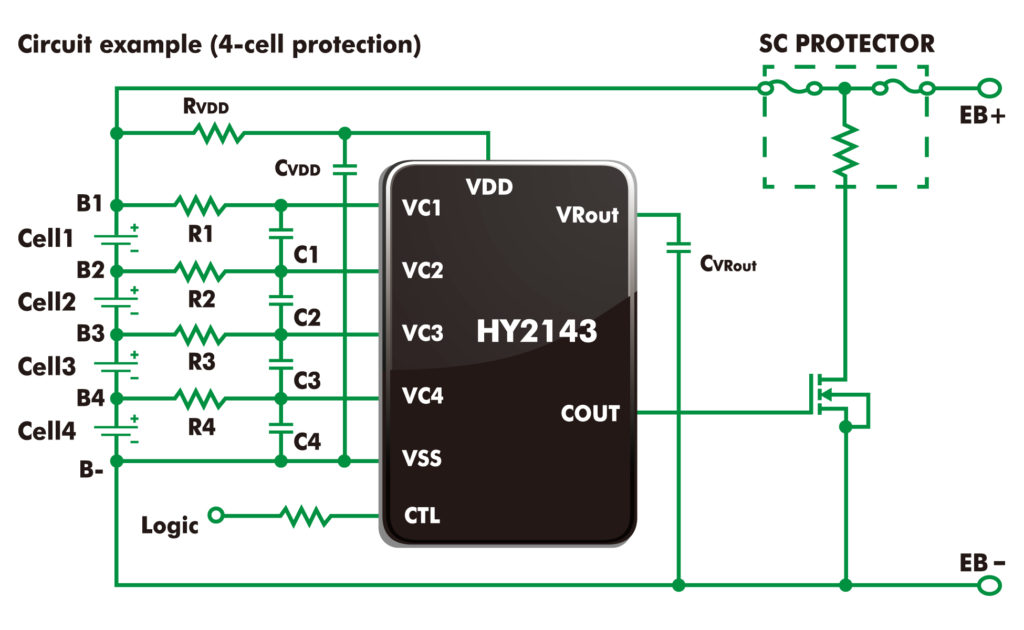
Product Features
- High-accuracy voltage detection circuit
- Delay time is set by internal circuit (external capacitor is not needed)
- Output logic: Active high CMOS output; the high level is 4.7V (typical) output from regulator
- utput logic active high maximum time: (optional; not-limited as default)
- Low current consumption
- Operation mode 5.0μA typ., 9.0μA max (VCelln = 3.9V)
- Shutdown mode 1: 4.5μA typ., 8.0μA max. (VCelln = 3.1V
- Shutdown mode 2: 0.6μA typ., 1.0μA max. (VCelln = 2.0V)
- LDO output circuit
- LDO output voltage 3.0V/3.3V typ. Accuracy: ±65mV
- LDO output current 2mA max
- Input voltage detection level:
- Voltage detection level (from VDD) 2.8V typ. Accuracy: ±1V
- High voltage resistant design: the absolute maximum rated value is 30V
- Wide operating temperature range: -40°C to +85°C
- Small package: DFN-2.0*2.0-8L
- Halogen free green product
Resources
| File Name | Description | File Manual |
|---|---|---|
| DS-HY2143 | HY2143 Series Chip Datasheet | DS-HY2143_EN.pdf |
| HY2143 Selection Guide | HY2143 Series Selection Guide | SelectionGuide_HY2143_EN.xlsx |