HY2151-GJ1C
Diagram
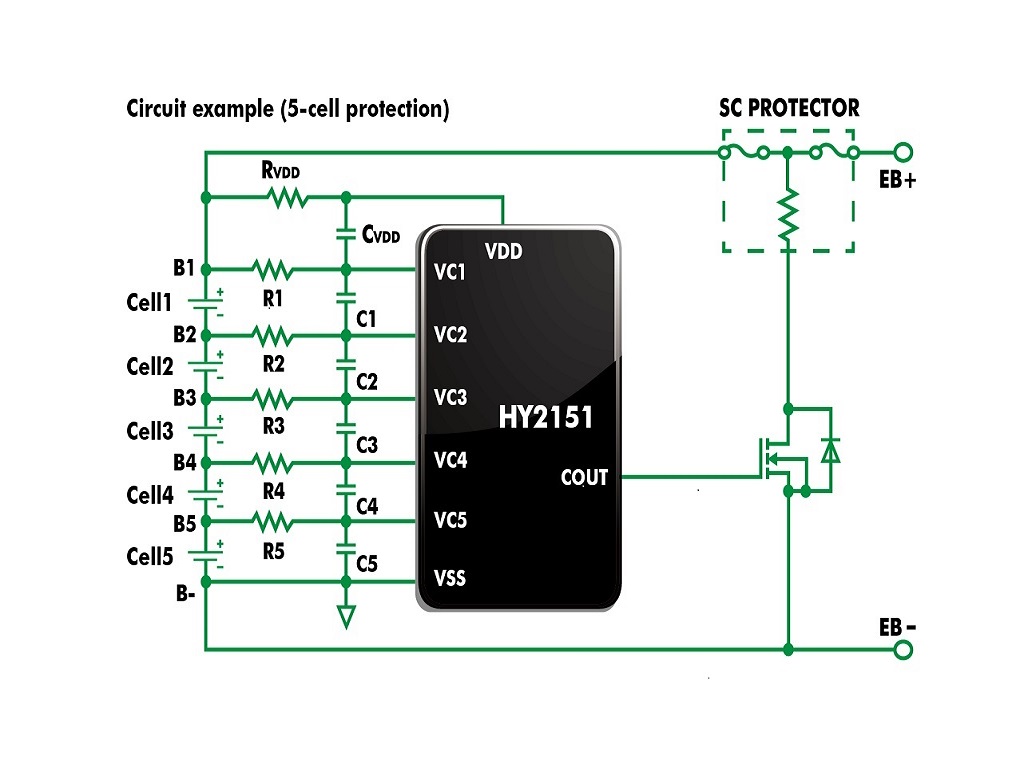
Product Features
- High -accuracy voltage detection circuit (n = 1, 2, 3, 4, 5)
- Overcharge detection voltage VCUn 4.0V to 5.0V Accuracy: ±25mV (25°C)
- Overcharge release voltage VCRn 3.8V to 5.0V Accuracy: ±50mV
- Delay time is set by internal circuit (external capacitor is not needed)
- Overcharge detection delay 1/2/4/6 s Accuracy: ±20%
- Built-in timer reset delay circuit
- Output is CMOS output Active "H"
- Output logic active high maximum time: Not Limited
- Low current consumption(25°C; n = 1,2,3,4,5)
- Operation mode(VCu = 4V)3.2μA typ.,5.0μA max
- Overdischarge mode(VCu = 2.3V)0.4μA typ.,1.0μA max
- High voltage resistant design: the absolute maximum rated value is 32V
- Wide operating temperature range:-40°C to + 85°C
- Small package:DFN8(1.97 * 2.46 mm)
- Halogen free green product
Resources
| File Name | Description | File Manual |
|---|---|---|
| DS-HY2151 | HY2151 Series Chip Datasheet | DS-HY2151_EN.pdf |
| HY2151 Selection Guide | HY2151 Series Selection Guide | SelectionGuide_HY2151.xlsx |